Best Practices for EMI PCB Design and Layout
Electromagnetic interference (EMI) is a critical challenge in PCB design, particularly when it comes to managing emi pcb effectively. Poor EMI management can lead to malfunctions and regulatory non-compliance. This article explores key strategies to control EMI in PCB layouts, helping you design reliable and compliant electronic devices.
Key Takeaways
- Understanding and controlling electromagnetic interference (EMI) is essential in PCB design to ensure signal integrity and compliance with regulatory standards.
- Key techniques for mitigating EMI include effective grounding, strategic component placement, and the use of decoupling capacitors and shielding methods.
- Conducting thorough EMC testing is vital for verifying compliance with regulations and ensuring reliable performance of electronic devices against EMI from external sources.
Understanding EMI in PCB Design

Electromagnetic interference, or electromagnetic interference EMI performance, is an electromagnetic disturbance that corrupts signal quality, leading to potential malfunctions in electronic devices. PCB designers must understand EMI and its management to ensure effective designs. Effective EMI control ensures that devices meet regulatory standards and function as intended, free from the disruptive influence of electromagnetic noise.
The impact of EMI on printed circuit boards (PCBs) can be profound. It can cause noisy disturbances and interference with signals, ultimately compromising the reliability of electronic devices. This interference can stem from various sources, including both conducted and radiated EMI, each presenting unique challenges that designers must address.
Controlling EMI from the start of PCB design is crucial. Adopting proactive design strategies helps designers avoid costly fixes later and meet stringent electromagnetic compatibility (EMC) requirements. As technology continues to advance, the importance of mitigating EMI will only grow, making it crucial for designers to stay ahead of the curve.
Major Sources of EMI in PCBs
Identifying major sources of electromagnetic interference in PCBs is the first step to mitigate its effects. EMI in PCBs primarily manifests in two forms: conducted EMI and radiated EMI. Each type has distinct origins and requires specific strategies to control.
Radiated EMI is generated from electromagnetic waves emitted by various devices, which can act like an antenna within the PCB layout. This type of EMI is particularly insidious as it can easily spread through the air, causing interference with other electronic equipment and electronic systems, which can generate EMI and electromagnetic radiation emitted and radiated emissions.
In contrast, conducted EMI is often introduced by power supplies that inject noise characteristics and ripple onto power rails, transferring unwanted high-frequency noise through capacitive coupling or electromagnetic fields.
High-frequency traces on PCBs also play a significant role in generating EMI within a specific frequency range. These traces can contribute to both radiated and conducted EMI by allowing electromagnetic radiation and coupling to other circuit components. Understanding these sources is crucial for PCB designers aiming to control EMI effectively and ensure the reliable performance of their electronic devices.
Techniques to Control EMI in PCB Layouts

Mitigating electromagnetic interference in PCB layouts requires a combination of strategic techniques. Effective shielding, for instance, involves using metal enclosures or conductive coatings to block electromagnetic radiation. Incorporating shielding, spacing, and twisted pair wires significantly reduces magnetic coupling and controls EMI.
Proper grounding techniques are another cornerstone of EMI control. Ground planes minimize the impact of conducted EMI by providing a low-impedance return path for currents. Decoupling capacitors placed between power and ground planes create low-impedance paths for return currents, aiding in EMI mitigation.
Component placement and trace separation play a pivotal role in minimizing EMI by:
- Grouping components by signal type (analog and digital) to reduce noise interference
- Maintaining a trace separation of at least three times the trace width to reduce crosstalk and unwanted coupling
- Using differential pairs for high-speed signals to cancel noise from external interference
- Reducing the length and area of signal return paths to minimize EMI in PCB layouts
The Role of Ground Planes in Reducing EMI

Ground planes are indispensable in the design of PCBs, serving as a crucial element in mitigating electromagnetic compatibility (EMC) problems. Ground planes minimize electromagnetic emissions and crosstalk by reducing ground inductance, enhancing overall signal integrity.
A larger ground area on a PCB leads to reduced ground inductance, which translates to lower electromagnetic emissions. In designs where full ground planes are not feasible, ground grids can serve as an effective substitute, particularly in two-layer PCBs, to help lower inductance.
Placing a ground plane beneath a signal trace effectively reduces EMI by:
- Minimizing the loop area for current, thereby reducing the potential for electromagnetic interference.
- Providing shorter return paths for signals, which minimizes loop inductance.
- Enhancing the electromagnetic compatibility performance of the PCB.
Importance of Power and Ground Planes
Power and ground planes are foundational to enhancing signal integrity and reducing electromagnetic interference in PCBs. A power plane distributes supply voltages evenly across the PCB, reducing voltage drops and improving EMC performance.
Thoughtful arrangement of pcb stack up layers is crucial. Placing power planes beneath ground planes optimizes the overall layout, thereby enhancing EMC performance and ensuring stable operation of the electronic device. Maintaining low impedance in power traces supports rapid current demands during device switching, maintaining signal integrity.
Careful planning of return current paths is vital, especially in mixed-signal PCB components designs. In high-frequency applications, capacitors should be placed near the power and ground pins of integrated circuits to minimize noise and preserve signal integrity. This approach ensures that the PCB performs reliably even under demanding conditions.
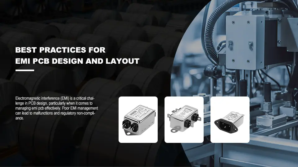
DOREXS PCB EMI Filters
DOREXS is a renowned provider of advanced PCB EMI filters, designed specifically to mitigate high-frequency electromagnetic interference in printed circuit boards. These filters are engineered to eliminate EMI, ensuring smooth operation of electronic devices in both AC and DC applications.
With a rated current capacity ranging from 1 to 20 amperes, DOREXS PCB filters are versatile and compact, making them easy to install on circuit boards. Moreover, DOREXS offers custom filter solutions to meet the specific requirements of different applications, ensuring optimal EMI mitigation for a wide range of electronic devices.
Effective Use of Decoupling Capacitors
Decoupling capacitors are essential in minimizing high-frequency noise, which is critical for achieving good EMC performance. These capacitors act as local energy buffers, stabilizing voltage levels close to integrated circuits and ensuring their proper functioning.
Proper placement of decoupling capacitors is crucial to minimize inductance and enhance high-frequency performance while avoiding performance degradation. Using multiple capacitors in parallel covers a wider frequency spectrum and reduces resonance issues in the power distribution network. In designs without power planes, placing at least one bypass capacitors for each active device reduces voltage drop and helps mitigate parasitic capacitance.
Decoupling capacitors are particularly important in clock circuits, where they help suppress noise along supply rails. Ensuring stable voltage levels and minimizing noise coupling, decoupling capacitors maintain the performance and reliability of sensitive components and clock signals.
Shielding Techniques for EMI Reduction

Board-level EMI shielding is a critical technique for reducing electromagnetic interference in PCB designs. The primary goal is to create a protective barrier around the PCB that contains electromagnetic emissions, thereby preventing EMI. Shielding absorbs and reflects radiation, ensuring electronic devices operate without interference, including board level shields.
Effective shielding methods include metal shielding cans, shielding compounds, and metalized enclosures. Using a Faraday cage or guard ring can further isolate the noisy environment within the PCB, enhancing overall electromagnetic compatibility.
Cable shielding effectively reduces EMI. Grounding cables at both ends significantly diminishes electromagnetic noise and ensures smooth operation of electronic devices. Appropriate shielding compounds and enclosures enhance EMI control effectiveness.
Designing High-Speed Signal Traces
Designing high-speed signal traces requires meticulous attention to detail to maintain signal integrity and minimize noise. Using 135° bends for signal traces, rather than 90°, minimizes signal distortion and improves performance, avoiding sharp bends. Length matching of traces is also necessary to achieve proper timing and avoid data skew in high-speed circuits.
Key practices for routing differential pairs and managing signal traces include:
- Routing differential pairs on the same layer and maintaining consistent impedance to prevent signal integrity issues.
- Keeping differential pairs close together to maintain consistent impedance and reduce electromagnetic interference.
- Maintaining increased spacing between signal traces, especially outside crowded regions, to diminish crosstalk.
Stitching capacitors should be used when routing signals over split planes to ensure proper return paths and mitigate noise. These techniques help design high-speed signal traces that perform reliably and efficiently.
EMC Testing and Compliance

EMC testing is crucial to ensure that electronic devices do not emit excessive EMI and maintain functionality when exposed to EMI from other devices. Compliance with EMC regulations and emc analysis is mandatory in many countries; non-compliance can result in fines or product seizures.
Procurement specifications often require stricter EMC compliance than regulatory standards, tailored to meet the specific needs of buyers. However, integrating multiple compliant components can present unexpected EMC challenges that may not meet regulatory requirements. It is essential for designers to conduct thorough EMC testing to identify and address any potential issues.
Ensuring EMC compliance avoids legal repercussions and guarantees that electronic products, including medical devices and cell phones, perform reliably under normal operation. By adhering to EMC standards, designers can achieve good EMC performance and ensure the success of their electronic devices in the market.
Summary
In summary, understanding and managing electromagnetic interference is crucial for PCB designers aiming to achieve good EMC performance. By identifying the major sources of EMI, implementing effective control techniques, and utilizing advanced components such as DOREXS PCB EMI filters, designers can significantly enhance the reliability and functionality of their printed circuit boards.
As technology continues to evolve, the importance of proactive EMI management will only increase. By applying the best practices outlined in this blog post, designers can ensure their PCBs meet regulatory standards, perform flawlessly, and stand the test of time. Embrace these strategies, and step confidently into a future where EMI is no longer a formidable adversary, but a controlled variable in your design process.
Frequently Asked Questions
What is EMI, and why is it important in PCB design?
EMI, or electromagnetic interference, is a disturbance that adversely affects the quality of signals in electronic devices. Its management is essential for compliance with regulatory standards and ensuring the reliable operation of these devices.
What are the major sources of EMI in PCBs?
The major sources of EMI in PCBs are conducted EMI from power supplies and radiated EMI from electromagnetic waves emitted by various devices. It is essential to address both to ensure optimal performance and compliance.
How can grounding techniques help in controlling EMI?
Grounding techniques significantly aid in controlling EMI by offering a low-impedance return path for currents, which enhances signal integrity and mitigates electromagnetic emissions. This ensures improved performance and reliability of electronic systems.
What are DOREXS PCB EMI filters, and how do they help?
DOREXS PCB EMI filters are specialized components that effectively reduce high-frequency electromagnetic interference in printed circuit boards for both AC and DC applications. By incorporating these filters, you can achieve improved signal integrity and reliability in your electronics.
Why is EMC testing important for electronic devices?
EMC testing is crucial as it verifies that electronic devices do not produce excessive electromagnetic interference (EMI) and can operate properly when subjected to EMI from other devices. Compliance with EMC regulations is essential to avoid legal repercussions and ensure product marketability.
Top Tips for Effective EMC Filter Design
Top Power Quality Solutions for Improved Energy Efficiency