How Grounding Impacts EMI Performance: A Practical Engineering Guide
Introduction
How grounding impacts EMI performance is fundamentally about controlling current return paths and reference potentials that determine whether your electronic devices pass or fail electromagnetic compatibility tests. Poor grounding design creates high impedance paths that allow noise currents to radiate efficiently, while proper grounding provides low impedance routes that contain electromagnetic interference within your system. This relationship between electrical grounding and electromagnetic interference emi directly affects both conducted and radiated emissions measured during CISPR, IEC, and FCC compliance testing.
The difference between passing EMC certification on the first attempt versus costly redesign cycles often comes down to how well you’ve implemented your grounding system at the PCB, enclosure, and cable level.
The difference between passing EMC certification on the first attempt versus costly redesign cycles often comes down to how well you’ve implemented your grounding system at the PCB, enclosure, and cable level.
What This Guide Covers
This guide examines practical grounding strategies for PCB ground planes, chassis and earth ground connections, cable shielding, and their measurable effects on conducted and radiated EMI in electronic systems. You’ll see specific examples for switching power supplies, motor drives, and high speed digital circuits, including how DOREXS EMI filters integrate with proper grounding to achieve reliable compliance. We focus on engineering decisions you can implement immediately, not theoretical electromagnetic field calculations or utility-scale power system grounding.
Who This Is For
This guide is designed for:
-
Hardware design engineers working on products requiring EMI/EMC compliance (EN 55032, CISPR 11)
-
Power electronics and motor control engineers struggling with radiated or conducted emissions failures
-
EMC/test engineers and technicians in pre-compliance labs
-
Advanced hobbyists designing PCBs for RF, switching regulators, or high speed logic
Whether you’re debugging a failing radiated emissions test or designing grounding from scratch, you’ll learn to connect specific grounding choices with concrete EMI behavior and test results.
Why This Matters
Failed EMC tests due to poor grounding can delay product launches by months, trigger expensive board respins, and cause unexpected system instability in the field. Grounding is often treated as an afterthought, yet small changes to ground plane design or proper integration of EMI filters like DOREXS single-phase and three-phase filters can mean the difference between first-time pass and multiple redesign cycles. The cost of fixing grounding issues late in development far exceeds the effort required to implement proper electrical grounding from the beginning.
What You’ll Learn:
-
How different grounding architectures (single point grounding, multipoint, hybrid) change EMI current flows and system performance
-
How PCB ground planes, splits, and via stitching affect high frequency noise and common mode interference
-
How chassis and earth ground connections influence both safety and electromagnetic compatibility
-
How cable and shield grounding choices impact radiated emissions and electrostatic discharge susceptibility
-
How to integrate DOREXS EMI filters with proper grounding to meet EMC standards reliably
-
Practical troubleshooting steps you can apply during your next design review
Understanding Grounding and EMI Fundamentals
Electromagnetic interference and grounding are inseparably linked because grounding defines the return paths and reference potentials that noise currents use to complete their circuits. Every current that flows in electronic equipment must return to its source through some conductive path—and these ground paths determine whether that current radiates as unwanted electromagnetic fields or stays contained within your system. Understanding this relationship provides the foundation for making informed grounding decisions that directly improve EMC performance.
What “Ground” Really Means in EMI Context
Ground in electronic circuits is fundamentally a current return path and voltage reference point, not automatically a connection to earth ground. In EMI contexts, we distinguish between signal ground (the 0V reference on your PCB), chassis ground (the metal enclosure), earth ground (connection to building electrical safety ground), and functional ground (the reference for normal circuit operation). At DC and low frequencies, these can often be treated as a single equipotential node, but at radio frequencies and during fast switching transients, each has distinct impedance characteristics that affect electromagnetic interference.
The crucial insight for EMI control is that high frequency currents will find the lowest impedance path back to their source, regardless of what you intended as the “ground” connection. A skinny grounding wire that works fine at 60 Hz becomes a high impedance obstacle at MHz frequencies, forcing noise currents to seek alternative return paths through stray capacitance, cable shields, or chassis structures—often creating the very radiation patterns that cause EMC failures.
The crucial insight for EMI control is that high frequency currents will find the lowest impedance path back to their source, regardless of what you intended as the “ground” connection. A skinny grounding wire that works fine at 60 Hz becomes a high impedance obstacle at MHz frequencies, forcing noise currents to seek alternative return paths through stray capacitance, cable shields, or chassis structures—often creating the very radiation patterns that cause EMC failures.
How EMI Currents Use Ground Paths
EMI manifests in two fundamental forms that interact differently with your grounding system: differential mode currents that flow in opposite directions on signal pairs, and common mode interference where currents flow in the same direction on multiple conductors relative to ground. Differential mode currents typically stay contained within well-designed circuits, but common mode currents seek to return through ground structures, chassis connections, and cable shields where they can easily radiate as electromagnetic fields.
The physics is straightforward: current loops create magnetic fields, and changing magnetic fields create electric fields that radiate. Your grounding system controls the size and impedance of these current loops. Large loop areas formed by poor ground paths create efficient antennas for electromagnetic radiation, while tight return paths immediately adjacent to signal conductors minimize both loop area and radiation. This is why a switching power supply with traces routed over a continuous ground plane typically radiates 20-30 dB less than the same circuit using narrow ground traces with detours around other components.
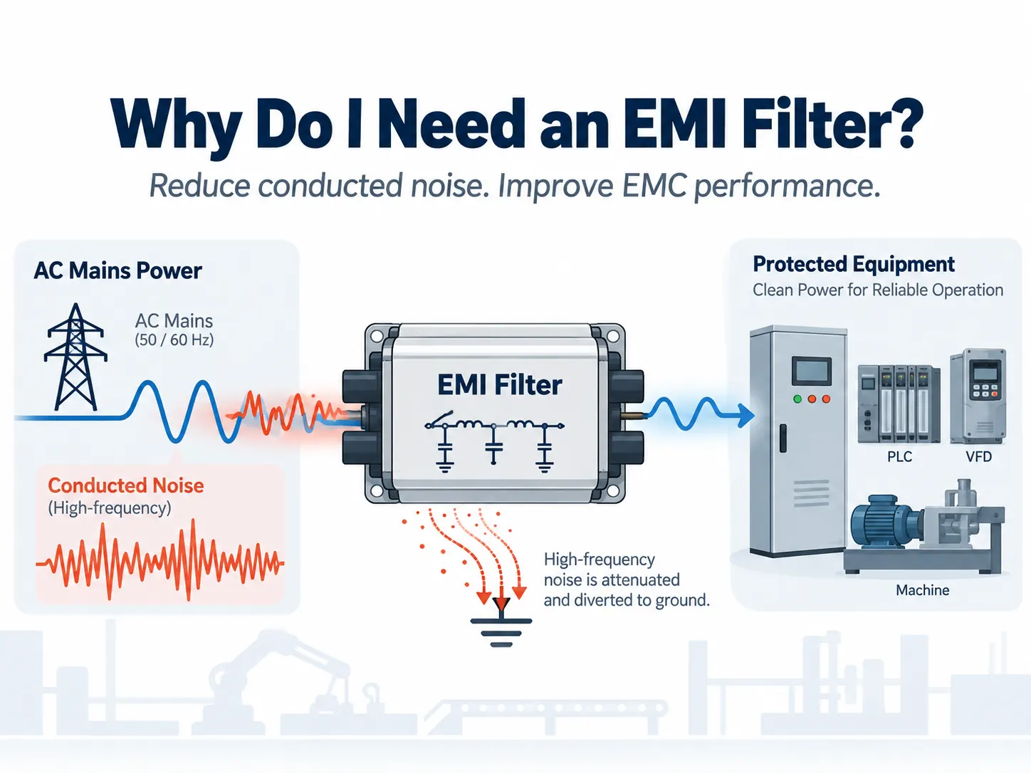
Common mode interference is particularly important because this is precisely what DOREXS EMI filters and similar products are designed to attenuate on power lines and signal interfaces. When your grounding system provides a low impedance path for these currents at the frequencies where they occur, filters can perform close to their theoretical insertion loss specifications.
How PCB Grounding Impacts EMI Performance
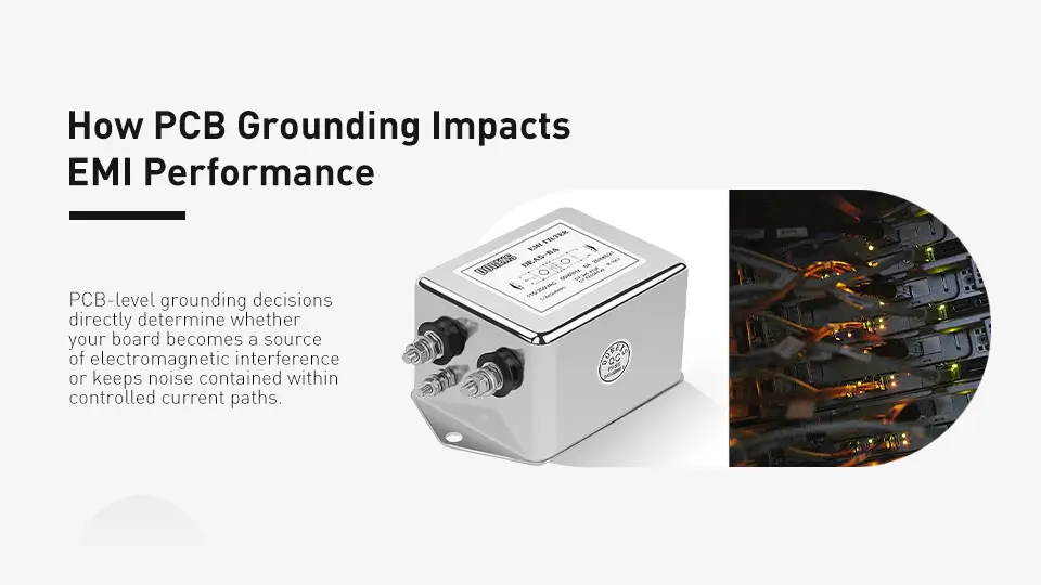
PCB-level grounding decisions directly determine whether your board becomes a source of electromagnetic interference or keeps noise contained within controlled current paths. Even the most sophisticated system-level EMI filters cannot compensate for fundamentally poor return path design at the PCB level, where fast switching edges first create the noise currents that must be managed. The key is understanding how different grounding approaches affect current flow patterns at the frequencies where EMI occurs.
Ground Planes vs Ground Traces
A continuous ground plane dramatically reduces both inductance and loop area compared to narrow ground traces or star-wired ground connections. While a typical PCB trace exhibits roughly 20 nanohenries per inch of inductance, a ground plane provides distributed return paths with much lower impedance at high frequency. Consider a switching converter operating at 100 kHz with 1 nanosecond edge times: the high frequency content extends well into the MHz range where that trace inductance becomes significant impedance.
The difference in EMI performance is measurable and substantial. A switching regulator laid out with skinny ground traces connecting various ground points might exhibit conducted emissions 15-25 dB higher than the same circuit implemented over a continuous ground plane. The ground plane allows high frequency return currents to flow directly underneath their corresponding signal traces, minimizing loop area and thus both magnetic field generation and radiated emissions.
This improvement in ground plane design directly enhances the effectiveness of EMI filters in your system. When DOREXS EMI filters or other suppression components are mounted with their ground terminals connected to a solid, low impedance plane rather than a narrow trace, they can achieve insertion loss performance much closer to their laboratory specifications.
Split Grounds: When They Help and When They Hurt
Splitting analog and digital grounds or separating noisy switching circuits from sensitive analog sections can reduce interference at low frequencies, but creates problematic return path discontinuities at high frequency. The common practice of connecting split ground regions at a single point works well for minimizing common impedance coupling of audio-frequency signals, but forces high frequency return currents to detour through that single connection point, often creating slot antennas that radiate efficiently.
A mixed-signal PCB with ADC circuits, for example, might benefit from separate analog and digital ground regions to prevent digital switching noise from coupling into sensitive analog inputs through shared ground impedance. However, if fast digital signals must cross between these regions, the return current cannot follow directly underneath the signal trace, forcing it to detour back to the single connection point. This enlarged current loop can increase radiated emissions significantly in the 30-300 MHz range where EMC compliance is measured.
The solution requires balancing frequency-dependent behavior: maintain separate ground regions for DC and low-frequency isolation while providing high-frequency connections (often through capacitors or ferrite beads) that allow RF return currents to follow more direct paths. In motor control applications, this might mean isolating the low-side gate drive returns from sensitive control circuits at DC while connecting them through ceramic capacitors for high-frequency return current flow.
Via Stitching, Return Paths, and Layer Stackup
Every high speed signal transition requires a local, low-inductance return path, and via stitching provides the connections necessary when signals change reference layers in multilayer PCBs. When a trace moves from one layer to another, its return current must also transition between ground or power planes. Without adequate stitching vias near the signal via, return currents are forced to find longer paths, increasing both inductance and radiated emissions.
A typical four-layer stackup with signal-ground-power-signal layers provides excellent EMI control when implemented correctly, with continuous reference planes under critical traces and stitching vias placed within a few millimeters of any layer transitions. The return current for a high speed trace on the top layer naturally flows in the ground plane immediately below, but if that trace transitions to the bottom layer, return current must move from the ground plane to the power plane through the nearest available via connection.
Professional EMC analysis of PCBs often reveals that seemingly minor return path disruptions—a missing via, a slot in the ground plane, or excessive spacing between signal and return paths—can increase radiated emissions by 10-20 dB in specific frequency bands. Even high-quality DOREXS EMI filters at the power input cannot fully compensate for poor return path design in switching circuits where nanosecond rise times create broadband noise spectra extending into the GHz range.
Key Points:
-
Continuous ground planes provide 15-25 dB better EMI performance than narrow ground traces
-
Split grounds require careful high-frequency stitching to prevent return path detours
-
Via placement near signal transitions is critical for maintaining controlled return paths
System, Chassis, and Cable Grounding Effects on EMI

System-level grounding decisions determine whether your carefully designed PCB EMI performance translates into EMC compliance when integrated into enclosures with cables and external connections. Many products with excellent PCB-level design still fail radiated emissions testing because chassis bonding, cable shield terminations, or earth ground connections create unintended current paths that turn the entire system into an efficient radiating antenna. Understanding these interactions allows you to maintain EMI control from component level through final system integration.
Chassis vs Signal Ground: Bonding Strategies
The relationship between your PCB signal ground and the metal enclosure or chassis fundamentally determines common mode current flow and thus radiated emissions. Chassis ground provides both mechanical support and electromagnetic shielding, but only when properly bonded to maintain the same potential as your signal ground reference across the frequency range where EMI occurs. Different bonding strategies create distinctly different current flow patterns with measurable impacts on EMC test results.
Single point bonding connects signal ground to chassis through one low-impedance connection, typically near the power entry point. This approach minimizes ground loops at power line frequencies but can create high impedance paths for high frequency noise currents that must travel the length of the PCB to reach the chassis connection. The result is often acceptable conducted emissions but elevated radiated emissions as noise currents find alternative return paths through stray capacitance and cable coupling.
Multiple point bonding uses several short, direct connections between signal ground and chassis, maintaining low impedance across a broader frequency range. While this may increase susceptibility to power line ground loops, it typically provides superior control of high frequency EMI by ensuring noise currents can reach chassis ground through the shortest available path. Many successful EMC designs use hybrid approaches: single point connection for DC and low frequency with additional capacitive or ferrite-coupled connections for high frequency return paths.
Cable and Shield Grounding Choices
Cable shields must be terminated to a stable, low-impedance reference to provide electromagnetic shielding, and poor shield grounding is among the most common causes of radiated emissions failures above 30 MHz. The fundamental principle is simple: a shield can only divert electromagnetic fields if noise currents induced in the shield have a low impedance path to flow without creating voltage drops that re-radiate. However, implementing this principle correctly requires understanding frequency-dependent tradeoffs.
Single-ended shield termination connects the cable shield at only one end, typically at the receiving equipment. This approach eliminates DC ground loops that can cause low-frequency hum and interference in audio and instrumentation systems, but provides limited high frequency shielding effectiveness because RF currents induced in the shield must travel the full cable length to find their return path. Above 10-30 MHz, where most EMC radiated emissions limits apply, single-ended shields often provide insufficient attenuation.
Double-ended shield termination connects the cable shield at both source and destination, creating a complete Faraday cage around the enclosed conductors. This provides excellent high frequency shielding but may create ground loops for DC and power-frequency currents flowing between different earth ground points in large installations. Many industrial and communications systems resolve this by using isolation transformers, differential signaling, or common mode chokes to break low frequency ground loops while maintaining high frequency shield continuity.
Ground Loops, Floating Grounds, and Noise Coupling
Ground loops occur when multiple return paths exist between equipment, allowing external electromagnetic fields to induce circulating currents that appear as noise in sensitive circuits. In large systems with multiple interconnected units, different earth ground connections can have significant potential differences due to fault currents, lightning strikes, or simply the resistance and inductance of building ground systems. These potential differences drive currents through signal and shield connections, creating both conducted and radiated interference.
Floating ground systems, common in medical equipment and precision instrumentation, avoid earth ground connections entirely to prevent ground loop currents and maintain patient safety isolation. While this eliminates ground loops, it can increase susceptibility to electrostatic discharge and capacitive coupling from external electromagnetic fields. The metal enclosures in floating systems can develop significant potential differences relative to nearby grounded equipment, potentially causing both EMI emissions and immunity problems.
A practical example from industrial control applications illustrates the impact: a motor drive system in a factory initially failed radiated emissions testing with cable radiation dominating above 100 MHz. Investigation revealed that the control cabinet door had paint preventing good electrical contact with the main cabinet structure. Adding a single braided grounding strap between door and cabinet frame reduced radiated emissions by 15 dB across the 30-300 MHz band by providing a controlled return path for noise currents that had previously coupled onto external cables.
This demonstrates how system-level grounding improvements work synergistically with component-level solutions. Even high-performance DOREXS EMI filters cannot achieve their full potential when mounted in systems with poor chassis bonding or uncontrolled cable shield terminations that allow noise currents to bypass the filter entirely.
Combining Grounding Design with EMI Filters for Best Performance

Proper grounding design and EMI filtering must be integrated from the beginning of your design process because filter effectiveness depends critically on having a stable, low-impedance reference for both common mode and differential mode attenuation. Even the highest quality EMI filters will underperform significantly when mounted with poor grounding connections, while thoughtfully designed ground structures can amplify filter effectiveness by ensuring noise currents flow through the intended attenuation paths rather than bypassing through parasitic coupling.
Step-by-Step: Integrating DOREXS EMI Filters into a Grounded System
When to use this: Apply this procedure when you have a power conversion system (switching supply, motor drive, or inverter) that needs to meet conducted emissions limits like EN 55011 or CISPR 32, or when pre-compliance testing shows emissions exceeding limits in the 150 kHz to 30 MHz range.
-
Map Noise Sources and Ground Paths: Identify all switching circuits, their fundamental frequencies and harmonics, and trace both differential mode (line to neutral) and common mode (line/neutral to ground) current paths. Use near-field probing or current clamps to measure actual noise current distribution and identify the dominant coupling mechanisms.
-
Select Appropriate DOREXS EMI Filter: Choose a DOREXS single-phase or three-phase filter with current rating adequate for your load and insertion loss characteristics that provide sufficient attenuation at your measured noise frequencies. Pay particular attention to common mode attenuation if cable radiation is a concern.For more foundational guidance, refer to the EMI filter circuit basics page.
-
Design Low-Impedance Filter-to-Chassis Bond: Mount the DOREXS filter so its metal case makes direct, wide-area electrical contact with your chassis ground structure. Avoid relying on threaded mounting hardware alone—use dedicated bonding straps or direct metal-to-metal contact with star washers to penetrate any oxidation or coating.
-
Separate Line and Load Side Routing: Maintain physical separation between unfiltered (line side) and filtered (load side) conductors to prevent high frequency coupling that can bypass the filter. Route input and output cables on opposite sides of the enclosure when possible, and avoid parallel routing that creates coupling capacitance.
-
Validate with Pre-Compliance Measurements: Use a line impedance stabilization network (LISN) and spectrum analyzer to verify that your combined grounding and DOREXS filter approach provides adequate margin below the applicable emission limits across the full 150 kHz to 30 MHz conducted emissions band.
The critical insight is that the filter’s ground terminal connection directly affects high frequency performance. A DOREXS filter with excellent laboratory specifications connected through 10 cm of wire to chassis ground may lose 20-30 dB of common mode attenuation above 1 MHz due to the wire inductance.
Comparison: Different Grounding Approaches for EMI Control
Grounding Strategy |
Frequency Range |
Typical Applications |
Conducted EMI Impact |
Radiated EMI Impact |
DOREXS Filter Integration |
| Single Point | DC to ~100 kHz | Audio equipment, precision instruments | Excellent for low-freq differential mode | Limited above 30 MHz | Filter ground connects to central star point |
| Multipoint | 1 MHz to GHz | Digital systems, switching converters | Good common mode control | Excellent high-freq performance | Filter case bonds directly to local |
| Hybrid | Full spectrum | Industrial controls, motor drives | Balanced performance | Good across all bands | Star point plus RF bypassing to chassis |
Single point grounding excels in applications where low frequency precision and ground loop elimination are priorities, but the increased path lengths for high frequency return currents limit EMI performance above 30 MHz. Multipoint grounding provides superior high frequency EMI control by minimizing inductance in return paths, but requires careful attention to low frequency ground loop management through isolation or common mode filtering.
Hybrid approaches often provide the best practical solution for complex systems by implementing single point behavior at DC and low frequencies while using capacitive coupling or ferrite connections to provide multipoint behavior at higher frequencies where EMI limits apply. When integrating DOREXS EMI filters into hybrid grounding systems, the filter’s common mode performance benefits from direct chassis bonding while differential mode performance depends more on the quality of the AC neutral return path.
The choice between these approaches should be driven by your system’s frequency content, physical size constraints, and the specific EMC standards you must meet, recognizing that EMI filters and grounding work as an integrated system rather than independent solutions.
Common Grounding-Related EMI Problems and How to Fix Them
Most EMI failures can be traced to a predictable set of grounding implementation mistakes that create uncontrolled current paths, turn system structures into efficient antennas, or prevent EMI filters from achieving their intended performance. Understanding these failure patterns allows you to diagnose EMC problems systematically and implement targeted solutions that address root causes rather than attempting broad-spectrum fixes that may miss the actual coupling mechanism.
Challenge 1: Passing Conducted Emissions on Mains Input
Product fails CISPR 32 or EN 55011 conducted emission limits around switching frequency harmonics (150 kHz to 10 MHz) despite having an EMI filter installed. This manifests as excess common mode current measured by the line impedance stabilization network (LISN), often with characteristic peaks at multiples of your switching frequency that exceed limits by 10-20 dB or more.
Solution: The most common cause is inadequate bonding between your EMI filter and chassis ground, creating inductance that reduces filter effectiveness at higher frequencies. Improve the protective earth (PE) and chassis connection of your DOREXS EMI filter by using the shortest, widest possible conductor—ideally direct metal-to-metal contact between filter case and mounting plate. Relocate the filter as close as possible to the mains entry point to minimize unfiltered conductor length. Physically separate line side and load side wiring to reduce parasitic coupling that can bypass the filter through stray capacitance.
These changes redirect common mode currents away from the mains conductors where they are measured by EMC test equipment. When common mode currents have a low impedance path through properly bonded filter components to chassis ground, they no longer appear as conducted emissions on the power lines.
Challenge 2: Failing Radiated Emissions Due to Long Cables
System passes conducted emissions tests but fails radiated measurements above 30 MHz, with I/O cables acting as efficient antennas that radiate noise generated by internal switching circuits. The failure typically shows broadband elevation across 30-300 MHz or specific peaks related to internal clock frequencies and their harmonics.
Solution: Implement proper 360-degree shield terminations where cables enter your enclosure, using conductive gaskets or backshells that bond cable shields directly to chassis ground with minimal inductance. Add ground plane stitching around connector areas and beneath relevant high speed signal traces on your PCB to ensure return currents flow in controlled paths rather than coupling onto cable shields. Apply DOREXS line filters or feedthrough capacitors on signal lines that carry switching noise, ensuring these filters are also properly grounded to chassis rather than connected through wires.
These measures reduce the common mode voltage between cable conductors and chassis that drives current flow on cable shields. When cables and chassis are at the same RF potential, the cables cannot function as effective radiating antennas. The combination of controlled return paths and proper filtering keeps noise currents local to the noise source rather than allowing them to propagate throughout the system.
Challenge 3: Susceptibility to ESD, EFT, and Surge Events
Product experiences random resets, communication errors, or component damage during IEC 61000-4-2 electrostatic discharge, IEC 61000-4-4 electrical fast transient, or IEC 61000-4-5 surge immunity testing. These failures often occur even when the primary protection components are properly rated and installed.
Solution: Re-evaluate your chassis and signal ground architecture to ensure that transient currents from ESD guns, burst generators, or surge simulators flow through defined, low-impedance paths that avoid coupling into sensitive circuit nodes. Implement continuous ground planes that extend under sensitive analog and digital circuits, with guard traces and controlled spacing around critical components. Add ground plane connections and stitching vias around areas where external interfaces connect to your PCB. Install DOREXS EMI and surge protection filters at power entries and high-exposure interfaces, ensuring these protective devices are integrated into your ground structure with short, direct connections.
The principle is that transient protection only works when the energy has a controlled path to dissipate without creating voltage differences across sensitive components. Improved grounding provides that controlled path by ensuring chassis ground, signal ground, and protective earth maintain the same potential during transient events, preventing the voltage differences that cause logic upsets or component stress.
Each of these solutions addresses the fundamental issue of controlling where currents flow under both normal and abnormal conditions, demonstrating that systematic grounding design prevents EMI problems rather than requiring reactive fixes after problems appear.
Coclusion and Pnractical Next Steps
How grounding impacts EMI performance comes down to a fundamental principle: electromagnetic interference follows the laws of physics, and current must return to its source through some path—your grounding design determines whether that path creates emissions problems or keeps noise contained within your system. Proper electrical grounding combined with appropriately selected EMI filters like those from DOREXS enables first-time EMC compliance and robust field performance by controlling current return paths from component level through final system integration.
The evidence from real-world EMC testing consistently shows that most emissions and immunity failures trace back to uncontrolled current paths created by inadequate ground plane design, poor chassis bonding, or incorrect cable shield terminations. These grounding issues can render even high-performance EMI filters ineffective, while proper grounding implementation allows filters to achieve their full theoretical insertion loss and provides the foundation for reliable electromagnetic compatibility.
To Get Started:
-
Audit your current design’s grounding architecture by sketching the actual current return paths for both normal operation and fault conditions, identifying any narrow traces, long connections, or discontinuous planes that create high impedance at radio frequencies.
-
Evaluate chassis bonding and shield terminations in your system, looking for connections made through small wires, painted surfaces, or single-point connections that may have adequate DC continuity but poor RF performance.
-
Review EMI filter integration by verifying that any DOREXS filters or other suppression components have low-inductance connections to your ground structure and are positioned to intercept noise currents before they can couple onto cables or radiate from large metal structures.
-
Plan pre-compliance validation focused specifically on how grounding changes affect EMI performance, using near-field probes and current measurements to verify that your design modifications actually redirect current flow as intended.
Related Topics: Consider exploring EMC shielding enclosure design, PCB stackup optimization for signal integrity, systematic EMI filter selection methodologies, and integrated surge protection strategies that complement your grounding implementation.
Additional Resources
International standards and regulations that define grounding requirements for EMC compliance include CISPR 11/32 for conducted and radiated emissions limits, the IEC 61000-4 series for immunity testing requirements, and EN 55032 for multimedia equipment standards that specify measurement methods and acceptable grounding practices.
DOREXS application engineering support provides design guidance on EMI filter selection, mounting techniques, and grounding best practices tailored to your specific application requirements, including reference designs that demonstrate proven integration approaches for power electronics and industrial control applications.
Technical references for deeper understanding include comprehensive EMC design handbooks that cover system-level electromagnetic compatibility, PCB-level grounding and layout techniques, and measurement procedures for validating grounding effectiveness using standard laboratory instruments.
Measurement tools for visualizing grounding impact on EMI include line impedance stabilization networks (LISNs) for conducted emissions testing, current probes for measuring actual noise current distribution, near-field probes for identifying radiation sources, and spectrum analyzers configured for EMC measurements that reveal how grounding changes affect emission spectra.
EMI Issues and Solutions in Medical Devices
What Is Leakage Current and Why It Matters : A Complete Guide to Electrical Safety