Switching Power Supply Output Filter-Complete Design Guide for Low-Noise DC Power
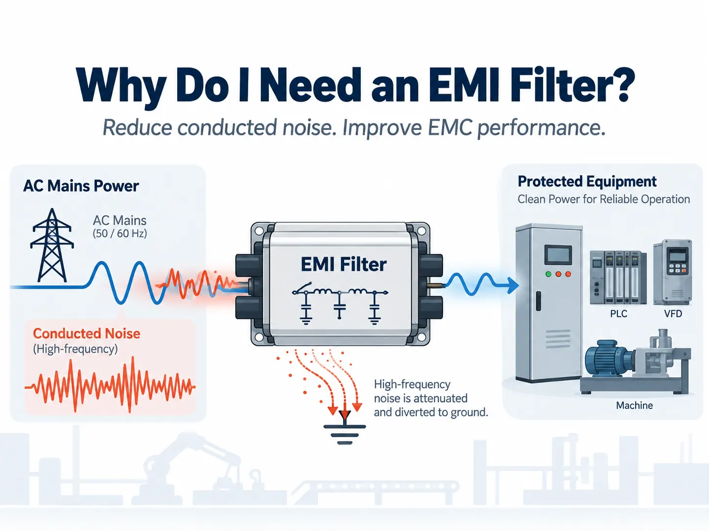
In today’s high-frequency switching power supplies, unwanted switching noise and ripple can wreak havoc on sensitive electronic circuits. Whether you’re designing precision analog systems, high-speed digital processors, or RF communications equipment, achieving clean DC power requires careful attention to output filter design. This comprehensive guide will walk you through everything you need to know about switching power supply output filters, from fundamental concepts to advanced implementation techniques.
Modern switching power supplies operate at frequencies ranging from 50 kHz to 2 MHz, generating significant high frequency noise that must be filtered before reaching sensitive loads. Without proper output filtering, this switching noise can cause measurement errors in precision instruments, introduce jitter in digital systems, and create unwanted interference in RF applications. The output filter serves as the critical barrier between the switching converter and your sensitive circuits, determining both power quality and system performance.

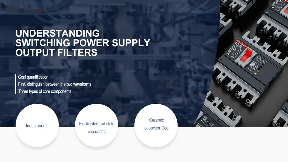
Understanding Switching Power Supply Output Filters
The switching power supply output filter serves a fundamental role in converting the chopped waveform produced by the switching converter into clean DC power suitable for sensitive loads. Unlike linear regulators that naturally produce smooth DC output, switching converters generate rectangular voltage pulses that contain both the desired DC component and unwanted high frequency harmonics.
The primary function of the output filter is to act as a low pass filter, allowing the DC and low frequency components to pass while attenuating high frequency switching noise. A well-designed filter reduces output ripple to acceptable levels, typically 5-100 mV peak-to-peak depending on the application requirements. Additionally, the filter improves transient response by providing local energy storage through output capacitors, helping maintain stable output voltage during sudden load changes.
Key performance metrics for switching power supply output filters include output ripple voltage, transient response time, efficiency, and noise rejection across the frequency spectrum. The cutoff frequency of the filter must be carefully selected to provide adequate attenuation at the switching frequency while maintaining fast transient response. Typical switching frequencies range from 50 kHz in high-power applications to 2 MHz in compact, high-efficiency designs using advanced semiconductors.
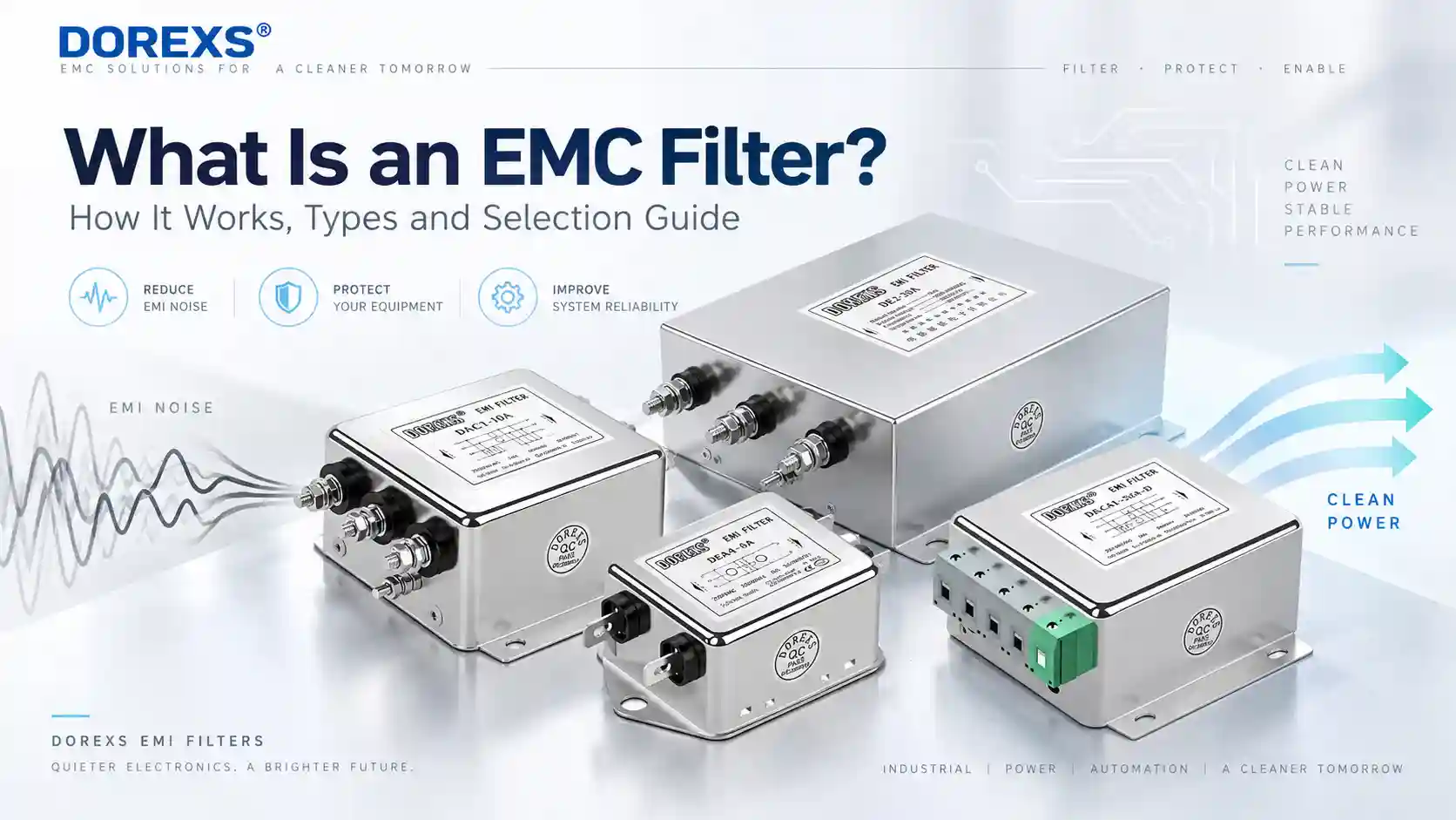
DOREXS switching power supply modules feature integrated output filtering designed to meet stringent noise and ripple specifications right out of the box. These modules combine optimized filter topologies with carefully selected components to deliver exceptional power quality while minimizing external component requirements.
Types of Output Filter Topologies
LC Filter Configurations
The LC filter represents the most common output filter topology in switching power supplies, combining a series inductor with a shunt capacitor to create an effective low pass filter. Single-stage LC filters typically use inductance values ranging from 0.5 μH to 2.2 μH, with the inductor chosen to have a high self resonant frequency well above the switching frequency. The series inductor blocks high frequency current ripple while the shunt capacitor provides a low impedance path for high frequency noise.
Multi-stage LC designs employ additional inductor-capacitor sections to achieve greater attenuation of switching noise. Each stage contributes approximately 40 dB per decade of frequency roll-off, allowing designers to achieve 60-80 dB total attenuation with two-stage designs. The additional complexity and component count must be weighed against the improved noise performance for each specific application.
Pi-Filter Topology
The pi filter configuration places an inductor between two capacitors, creating enhanced noise suppression compared to simple LC designs. This topology is particularly effective for applications requiring ultra-low output noise, such as precision analog circuits and RF applications. The input capacitor (C1) provides initial high frequency bypassing, while the inductor blocks switching current and the output capacitor (C2) provides final filtering and local energy storage.
Pi filters can achieve 10-20 dB better attenuation than equivalent LC filters, making them ideal for demanding applications where sub-millivolt ripple is required. The trade-off comes in increased component count, larger PCB footprint, and higher cost compared to simple LC implementations.
RC Second-Stage Filters
For low-current applications under 50 mA, RC filters can provide additional high frequency attenuation as a second stage following the main LC filter. The resistor value typically ranges from 1-10 ohms, chosen to provide adequate filtering without excessive voltage drop under load. RC filters are particularly effective at attenuating very high frequency noise above 10 MHz that may pass through the main LC filter.
However, RC filters dissipate power and reduce efficiency, making them unsuitable for high-current applications. The resistive element also degrades load regulation and transient response, limiting their use to auxiliary rails and low-power circuits.
Ferrite Bead Filters
Ferite beads provide excellent attenuation of high frequency noise above 100 MHz, making them valuable for suppressing conducted emissions and improving EMI performance. These components present high impedance (100-300 ohms) at frequencies above 100 MHz while maintaining low DC resistance. Ferrite beads are often used in conjunction with ceramic capacitors to create effective high frequency filters.
The DC current rating of ferrite beads must be carefully considered, as excessive current can cause core saturation and reduced filtering effectiveness. Multiple parallel beads may be required for high-current applications, or larger cores with higher saturation current ratings.
DOREXS offers integrated filter solutions that combine multiple topologies within compact power modules, providing optimized performance without the complexity of discrete component selection and layout optimization.
Component Selection and Design Calculations
Inductor Selection
Proper inductor selection is critical for effective output filtering, with inductance values typically ranging from 0.5 μH to 2.2 μH depending on the switching frequency and ripple current requirements. The inductor must have a high self resonant frequency (SRF), ideally at least 10 times the switching frequency, to maintain effective filtering performance. Low DC resistance minimizes power loss and voltage drop, while adequate saturation current rating prevents core saturation under peak load conditions.
The inductor value can be calculated using the relationship between switching frequency, acceptable ripple current, and output voltage. For a buck converter, the inductor value L = (Vin - Vout) × D / (f × ΔIL), where D is the duty cycle, f is the switching frequency, and ΔIL is the desired ripple current. Higher inductance values reduce ripple current but increase transient response time and component size.
Core material selection impacts both performance and cost, with ferrite cores providing good high frequency characteristics and powder cores offering better saturation performance. Shielded inductors reduce radiated emissions but may have higher cost and larger size compared to unshielded alternatives.
Capacitor Sizing
Output capacitor selection involves balancing ripple voltage requirements, transient response, and cost considerations. For achieving 5-20 mV peak-to-peak ripple, the capacitor value can be estimated using C = ΔIL / (8 × f × ΔVr), where ΔIL is the inductor ripple current and ΔVr is the acceptable ripple voltage. This calculation provides a starting point, with additional capacitance often required for transient response.
The equivalent series resistance (ESR) of output capacitors significantly impacts high frequency filtering performance. Low ESR ceramic capacitors (X7R dielectric) provide excellent high frequency bypassing but may require additional electrolytic capacitance for bulk energy storage. Aluminum electrolytic capacitors offer high capacitance per cost but have higher ESR and limited high frequency performance.
Controlled ESR can actually benefit filter stability by providing natural damping of resonant peaks. The optimal ESR value depends on the specific filter design and load characteristics, typically ranging from 10-100 milliohms for most applications.
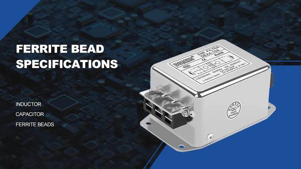
Ferrite Bead Specifications
When incorporating ferrite beads for high frequency noise suppression, the impedance characteristics must match the application requirements. Typical specifications include 100-300 ohms impedance at 100 MHz, with the impedance curve tailored to provide maximum attenuation in the frequency range of concern. The DC current rating must exceed the maximum load current with appropriate derating for temperature and aging effects.
Ferrite bead selection requires careful attention to the impedance vs. frequency curve, as some designs may exhibit resonant peaks that could amplify noise at specific frequencies. Multi-hole cores or cascaded single beads can provide broader frequency coverage and higher impedance when needed.
DOREXS provides comprehensive component recommendations and pre-validated filter designs that eliminate the guesswork in component selection. These designs have been tested across temperature, load, and frequency ranges to ensure reliable performance in demanding applications.
Damping Techniques for Stable Filter Response
Parallel Resistor Damping
Parallel resistor damping involves adding small resistance values (1-10 ohms) across output capacitors to control resonant peaks and prevent oscillations in the filter response. This technique is particularly important when using low-ESR ceramic capacitors that may not provide sufficient natural damping. The damping resistor value must be carefully selected to provide adequate damping without excessive power dissipation or degraded transient response.
The optimal damping resistance can be calculated based on the filter’s characteristic impedance and desired damping factor. For critical damping, the resistance should approximately equal the characteristic impedance Z = √(L/C) of the LC filter. Higher resistance values provide more damping but increase power loss, while lower values may not adequately suppress resonant peaks.
Temperature effects must be considered when selecting damping resistors, as resistance values can drift significantly over temperature. Metal film resistors provide better stability than carbon compositions, while precision thin-film devices offer the best temperature coefficient for critical applications.
RC Damping Networks
Series RC networks across filter inductors provide an alternative damping approach that can be more effective for certain filter designs. The RC network creates a parallel path for high frequency currents while the resistor provides damping at the filter’s resonant frequency. Typical values range from 1-10 ohms for the resistor with 0.1-1 μF for the capacitor, adjusted based on the specific filter characteristics.
RC damping networks are particularly effective for multi-stage filters where each LC section may have different resonant frequencies requiring individual damping. The additional complexity must be weighed against the improved stability and reduced ringing in the filter’s step response.
Critical Damping Calculations
Achieving critical damping requires careful balance between stability and transient response. The damping factor ζ should be maintained between 0.7-1.0 for most applications, providing good stability without excessive overshoot or settling time. Mathematical analysis using the filter’s transfer function helps optimize damping component values for specific performance requirements.
Computer simulation tools can model the complete filter response including parasitic elements and component tolerances. This analysis helps identify potential stability issues before hardware implementation and allows optimization of damping networks for best overall performance.
DOREXS pre-damped filter configurations eliminate the complexity of damping network design by incorporating optimized damping elements directly into the power module design. These solutions provide plug-and-play performance with guaranteed stability across all operating conditions.
Advanced Damping Methods
Snubber Circuits
Snubber circuits provide targeted damping of switching transients and high frequency oscillations by placing RC networks across switching elements or filter components. These circuits absorb energy during switching transitions and prevent voltage overshoots that could stress components or generate additional noise. Snubber design requires careful consideration of the energy levels involved and appropriate power ratings for the resistive elements.
Controlled ESR Capacitors
Specially designed capacitors with controlled ESR characteristics can act as integrated damping elements, eliminating the need for external damping components. These capacitors combine the bulk capacitance needed for filtering with precisely controlled resistance to provide optimal damping. The approach simplifies circuit design while maintaining excellent performance.
Active Damping Using Feedback Control Loops
Digital control loops can implement active damping by monitoring the filter response and adjusting switching parameters to suppress resonances. This advanced technique allows real-time optimization of filter performance but requires sophisticated control algorithms and fast digital signal processing capabilities.
Multi-Stage Damping for High-Performance Applications
Complex filter designs may require different damping techniques for each filter stage, with careful attention to the interaction between stages. Multi-stage damping can achieve exceptional noise performance while maintaining stability, but requires detailed analysis and careful component selection.
PCB Layout Considerations for Effective Filtering
Proper PCB layout is essential for realizing the full potential of switching power supply output filters. Poor layout can introduce parasitic inductance and capacitance that degrades filter performance and may even cause instability. The ground plane design forms the foundation of effective filtering, requiring a solid copper pour to provide a low impedance return path for high frequency currents.
Component placement directly affects filter performance through parasitic effects and coupling between components. Filter inductors should be positioned to minimize coupling with other magnetic components, while filter capacitors should be placed as close as possible to the switching converter output. Loop areas must be minimized to reduce parasitic inductance, which can significantly impact high frequency filtering effectiveness.
Via stitching between ground layers helps maintain low impedance ground connections, particularly important in multi-layer PCB designs. The layer stackup should consider both signal integrity and EMI performance, with careful attention to the placement of switching nodes and sensitive analog circuits. Power and ground planes should be designed with adequate width and minimal gaps to support high frequency current flow.
Long wire runs and perfboard layouts can introduce significant parasitic inductance that degrades filter performance. Each inch of wire or trace adds approximately 10-20 nH of inductance, which can resonate with filter capacitors and create unwanted peaks in the frequency response. Professional PCB layouts with controlled impedance traces and proper ground planes are essential for high-performance applications.
DOREXS provides comprehensive reference designs and layout guidelines that have been validated through extensive testing and simulation. These reference designs demonstrate optimal component placement, routing techniques, and layer stackup configurations for maximum filter effectiveness.
Frequency Response and Performance Analysis
Understanding the frequency response characteristics of switching power supply output filters is crucial for optimizing performance and ensuring stability. Bode plot analysis reveals both the magnitude and phase response across the frequency spectrum, allowing designers to identify potential resonances and verify adequate attenuation at the switching frequency and its harmonics.
The filter cutoff frequency should be selected to provide at least 40 dB attenuation at the switching frequency while maintaining adequate transient response for load step changes. A cutoff frequency approximately one-tenth of the switching frequency typically provides a good balance between filtering effectiveness and dynamic response. However, specific applications may require different trade-offs based on noise sensitivity and transient requirements.
Resonance control becomes critical when using multiple filter stages or when parasitic elements create unintended resonant circuits. The filter’s transfer function must be analyzed to identify all resonant frequencies and ensure adequate damping at each resonance. Undamped resonances can actually amplify noise at specific frequencies, degrading rather than improving overall performance.
Measurement techniques using spectrum analyzers and oscilloscopes provide essential verification of filter performance in actual circuits. Spectrum analysis reveals the noise floor and harmonic content across a wide frequency range, while time-domain measurements show transient response and settling behavior. Near-field EMI probes can identify localized noise sources and verify the effectiveness of filtering techniques.
Professional measurement setups require careful attention to measurement bandwidth, probe loading effects, and ground loop elimination. High-frequency noise measurements are particularly sensitive to measurement technique, and proper procedures are essential for accurate results.
DOREXS provides detailed filter characterization data and performance specifications based on professional test equipment and standardized measurement procedures. This data includes frequency response plots, transient response characteristics, and EMI performance under various operating conditions.
Application-Specific Filter Design
Audio Applications
Audio applications demand ultra-low noise performance with output ripple specifications often below 1 mV RMS across the audio frequency range. These stringent requirements typically necessitate multi-stage filtering with carefully optimized component selection. Low-noise linear post-regulators may be required following the switching stage to achieve the necessary noise floor for high-end audio equipment.
The frequency response of audio power supply filters must consider both audible frequencies (20 Hz to 20 kHz) and ultrasonic noise that could affect sensitive analog circuits. Ceramic capacitors with low microphonic effects and film capacitors for critical analog stages help maintain signal integrity in demanding audio applications.
Digital Circuits
Digital circuits generate significant switching noise at fundamental clock frequencies and harmonics extending well into the hundreds of megahertz range. Output filters must provide adequate attenuation at 100 MHz and above to prevent interference with high-speed digital signals. Multiple bypass capacitors with different values and types may be required to address the broad frequency spectrum of digital noise.
The transient response requirements for digital circuits are often more demanding than for analog applications, as rapid current changes during logic transitions must be supplied without significant voltage droop. Low-ESR capacitors and careful attention to current loops help maintain stable power delivery during high-speed switching.
RF Applications
RF applications require exceptional attention to conducted and radiated emissions that could interfere with sensitive receivers. Filter design must consider not only power supply noise but also the potential for filter components to act as antennas or transmission lines at RF frequencies. Shielded inductors and careful PCB layout help minimize radiated emissions.
The impedance characteristics of filter components at RF frequencies may differ significantly from their low-frequency behavior. Parasitic resonances in filter capacitors or inductors can create unwanted coupling paths that degrade RF performance. Component selection and layout must consider these high-frequency effects.
Medical Devices
Medical device applications must meet strict EMC and safety standards while often requiring exceptional noise performance for sensitive measurement circuits. IEC 60601 and similar standards specify rigorous testing requirements for conducted and radiated emissions. Filter designs must be validated through formal compliance testing to ensure regulatory approval.
Safety considerations for medical devices may require specific component certifications, creepage and clearance distances, and fault tolerance. Redundant filtering or fail-safe designs help ensure patient safety even under component failure conditions.
DOREXS offers specialized filter modules designed specifically for medical, audio, RF, and other demanding application domains. These modules combine optimized filtering performance with the necessary certifications and documentation for regulatory compliance.
Simulation and Verification Methods
SPICE Simulation Setup
SPICE simulation provides powerful tools for analyzing switching power supply output filter performance before hardware implementation. Proper simulation setup requires accurate models for all components including parasitic elements that significantly affect high-frequency behavior. Inductor models must include DC resistance, AC losses, and parasitic capacitance, while capacitor models should incorporate ESR, ESL, and voltage/temperature dependencies.
Transient analysis reveals the filter’s response to load step changes and switching transients, helping optimize component values for best dynamic performance. AC analysis provides frequency response data equivalent to network analyzer measurements, allowing detailed evaluation of filter characteristics across the frequency spectrum. Monte Carlo analysis can evaluate the effects of component tolerances on filter performance and identify critical parameters requiring tight control.
Component Modeling
Accurate component modeling is essential for meaningful simulation results, particularly at high frequencies where parasitic elements dominate behavior. Real-world inductors exhibit self-resonant frequencies due to parasitic capacitance, while capacitors show increasing impedance above their self-resonant frequency due to parasitic inductance. These effects must be included in simulation models to predict actual circuit performance.
Vendor-provided SPICE models often include detailed parasitic information based on actual component measurements. When vendor models are not available, simplified equivalent circuits can be constructed using datasheet information and general guidelines for parasitic values. However, hardware verification remains essential for
confirming simulation predictions.
Load Step Response Testing
Load step response testing evaluates the filter’s ability to maintain stable output voltage during rapid current changes. Test procedures typically apply step changes representing 10-90% of the maximum load current while monitoring output voltage deviation and recovery time. The results reveal the effectiveness of output capacitance and help optimize component selection for specific transient requirements.
Proper test setup requires careful attention to measurement bandwidth, probe placement, and load switching techniques. High-speed current sources or electronic loads provide controlled step changes, while differential probes minimize measurement artifacts that could mask actual performance.
EMI Pre-Compliance Testing
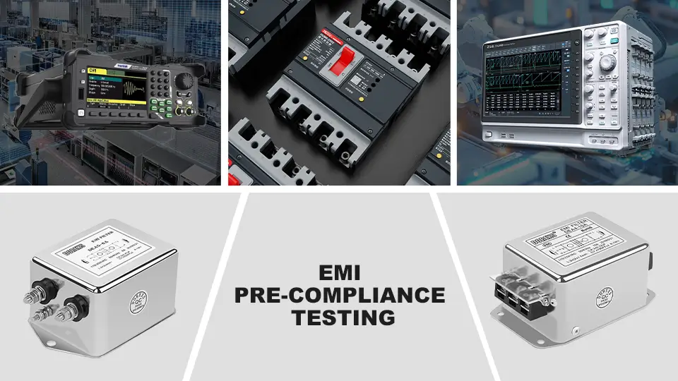
EMI pre-compliance testing using near-field probes helps identify noise sources and evaluate filter effectiveness before formal compliance testing. Near-field measurements can locate specific circuit areas generating excessive emissions and verify the effectiveness of filtering modifications. This approach allows iterative design improvements at much lower cost than formal EMI testing.
Line impedance stabilization networks (LISN) provide standardized measurement conditions for conducted emissions testing, while appropriate antennas and test distances are required for radiated emissions measurements. Understanding the test requirements and setup procedures helps ensure successful formal compliance testing.
DOREXS provides comprehensive simulation models and design verification tools that have been validated against extensive hardware testing. These tools help accelerate the design process while ensuring reliable performance in final applications.
Common Design Challenges and Solutions
Capacitor Aging and Drift
Ceramic capacitors used in switching power supply output filters can experience significant capacitance changes due to DC bias effects, temperature variations, and aging. X7R and X5R dielectrics maintain better stability than Y5V types but still show 15-20% capacitance reduction under rated voltage conditions. Design margins must account for these variations to ensure adequate filtering performance over the product lifetime.
Temperature effects can cause additional capacitance changes, particularly in ceramic dielectrics where capacitance may vary by ±15% over the operating temperature range. Aluminum electrolytic capacitors also show significant temperature dependence and have limited lifetime at elevated temperatures. Component selection and derating help minimize these effects.
Aging effects in electrolytic capacitors can cause both capacitance decrease and ESR increase over time, gradually degrading filter performance. Regular monitoring of critical power supplies and preventive replacement schedules help maintain system reliability in long-term applications.
Inductor Saturation
Filter inductors can experience core saturation under high current conditions, leading to reduced inductance and degraded filtering performance. Saturation current ratings must exceed the peak current including both DC load current and AC ripple current with appropriate safety margin. Temperature effects on core material can further reduce saturation current, requiring additional derating for high-temperature operation.
Powder core materials generally provide better saturation characteristics than ferrite cores but may have higher core losses at high frequencies. The choice between core materials involves trade-offs between saturation performance, high-frequency losses, and cost. Distributed gap cores help minimize fringing field effects while maintaining good saturation performance.
Current monitoring circuits can provide early warning of approaching saturation conditions, allowing protective action before performance degradation occurs. Parallel inductor configurations can increase current handling capability but require careful matching to ensure equal current sharing.
Filter Instability and Oscillation
Filter instability can manifest as oscillations at the filter’s resonant frequency, particularly when using low-ESR capacitors with insufficient damping. These oscillations can interfere with the switching converter’s control loop and create additional noise rather than reducing it. Proper damping techniques and careful analysis of the complete system transfer function help prevent instability.
Parasitic elements in the PCB layout can create unintended resonant circuits that contribute to instability. Long traces, inadequate ground planes, and poor component placement can introduce parasitic inductance and capacitance that affect filter behavior. Professional PCB layout practices and simulation verification help identify and eliminate these issues.
The interaction between the output filter and the switching converter’s control loop requires careful analysis to ensure overall system stability. The filter’s impedance characteristics affect the control loop’s phase and gain margins, potentially causing instability if not properly considered during design.
Cost Optimization
Achieving target performance specifications while minimizing cost requires careful balance of component selection and circuit complexity. Higher-value inductors and capacitors generally cost more but may allow simpler single-stage designs versus more complex multi-stage approaches using smaller components. Volume considerations and supplier relationships also significantly impact component costs.
Standardization on common component values across multiple designs can provide volume discounts and simplified inventory management. However, this approach may not always yield optimal performance for every application. The trade-off between standardization benefits and performance optimization must be evaluated for each specific situation.
DOREXS technical support and design consultation services help optimize filter designs for both performance and cost objectives. Experienced applications engineers can recommend proven solutions that meet specifications while minimizing component costs and design complexity.
Modern Trends and Future Developments
GaN and SiC Devices
The adoption of gallium nitride (GaN) and silicon carbide (SiC) power semiconductors is enabling switching frequencies up to 10 MHz, dramatically reducing the size requirements for output filter components. Higher switching frequencies allow smaller inductors and capacitors while maintaining equivalent filtering performance, supporting the trend toward more compact power solutions.
However, the higher switching frequencies also create new challenges for filter design, as parasitic elements become more significant and EMI considerations extend to much higher frequencies. Component selection must consider performance characteristics well beyond traditional switching frequencies, and PCB layout becomes even more critical for maintaining filter effectiveness.
The faster switching transitions of wide-bandgap devices can generate more severe EMI issues despite the smaller filter components, requiring careful attention to layout and possibly additional high-frequency filtering stages. Balancing the benefits of higher switching frequencies with the challenges of increased EMI requires sophisticated design approaches.
Digital Control Loops
Digital control systems are enabling adaptive filtering techniques that can optimize filter performance in real-time based on operating conditions. Variable switching frequencies, adaptive damping, and load-dependent filter characteristics become possible with sophisticated digital control algorithms. These techniques can provide optimal performance across varying load and line conditions.
Digital implementations also allow more complex control strategies such as predictive control and multi-variable optimization that consider both power conversion efficiency and filter performance simultaneously. However, the increased complexity requires significant digital signal processing capabilities and sophisticated software development.
Integrated Power Modules
The trend toward integrated power modules combines switching converters, output filtering, and control circuitry in compact packages that simplify system design and improve performance. These modules can optimize the interaction between switching and filtering elements while providing guaranteed performance specifications and regulatory compliance.
Integrated magnetics techniques allow combining switching transformers and output inductors in single magnetic structures, further reducing size and cost while potentially improving performance through coupled magnetic effects. However, these approaches require sophisticated magnetic design and may limit flexibility for specific applications.
AI-Assisted Design
Artificial intelligence and machine learning techniques are beginning to impact power supply filter design through automated component selection, layout optimization, and performance prediction. AI algorithms can analyze vast databases of design examples and component characteristics to suggest optimal solutions for specific requirements.
Machine learning approaches can also help predict component aging effects and optimize designs for long-term reliability. However, these techniques require extensive training data and validation to ensure reliable results in practical applications.
DOREXS is actively developing next-generation power solutions that incorporate advanced filtering capabilities with intelligent control systems. These solutions combine proven filtering techniques with modern digital control and monitoring capabilities to provide exceptional performance and reliability.
Conclusion
Designing effective switching power supply output filters requires careful consideration of component selection, circuit topology, layout techniques, and application-specific requirements. The fundamental principles of low-pass filtering remain constant, but implementation details vary significantly based on performance specifications, cost targets, and regulatory requirements.
Modern trends toward higher switching frequencies and integrated solutions offer opportunities for more compact and efficient designs but also create new challenges for EMI control and high-frequency performance. Success requires balancing theoretical understanding with practical implementation experience and thorough verification testing.
DOREXS continues to lead the industry in developing innovative filtering solutions that combine proven design principles with advanced technologies. Whether you need standard catalog products or custom engineered solutions, DOREXS technical experts can help optimize your switching power supply output filter design for exceptional performance and reliability.
The investment in proper output filter design pays dividends in system performance, regulatory compliance, and long-term reliability. By following the principles and techniques outlined in this guide, engineers can achieve the clean, stable power required for today’s demanding electronic applications.
Top Power Quality Solutions for Improved Energy Efficiency
DC Noise Filter - Complete Guide to Power Supply Noise Suppression