Common EMC Test Failures and How to Avoid Them
Introduction
EMC test failures affect 50-80% of electronic products during initial compliance testing, with some sectors like medical devices experiencing failure rates exceeding 90% on first submission. These failures result from predictable design oversights in power supply filtering, PCB layout, and shielding implementation that can be prevented through systematic design practices and pre compliance testing.
EMC testing validates that electronic products neither emit excessive electromagnetic interference nor suffer from immunity problems when exposed to external RF energy sources.
EMC testing validates that electronic products neither emit excessive electromagnetic interference nor suffer from immunity problems when exposed to external RF energy sources.

What This Guide Covers
This guide examines the seven most frequent EMC failure categories in emissions testing and immunity tests, plus specific prevention techniques for conducted emissions (150kHz-30MHz), radiated emissions (30MHz-6GHz), and ESD testing. We focus on practical design solutions rather than theoretical compliance standards.
Who This Is For
This guide targets electronics engineers, product managers, and compliance teams preparing products for EMC certification. Whether you’re troubleshooting failed test reports or designing new products for commercial environments, you’ll find actionable prevention strategies and troubleshooting methods.
Why This Matters
EMC failures can delay product launches by 3-6 months and increase development costs by 20-50% due to redesign requirements, additional test lab sessions, and component changes. Early identification and prevention of common failure modes eliminates these costly delays.
What You’ll Learn:
- Root causes of conducted and radiated emissions failures
- PCB layout practices that prevent immunity testing failures
- Power supply and cable management techniques for compliance
- Step-by-step pre compliance testing procedures using basic test equipment
- Quick fixes versus design changes for common emc failures
- Integration strategies for EMI filter solutions including DOREXS products
Understanding EMC Test Requirements and Common Failure Points
EMC testing consists of emissions testing to measure unintended RF energy output and immunity testing to verify device operation under electromagnetic stress.
Emissions testing covers conducted emissions from 150kHz to 30MHz measured through power line impedance stabilization networks (LISN), plus radiated emission testing from 30MHz to 6GHz using calibrated receiving antenna systems in semi-anechoic chambers. Immunity tests include ESD testing at 4kV-15kV levels, RF immunity sweeps, and surge testing to verify the device continues normal operation.
Products fail because design teams often treat EMC requirements as an afterthought rather than integrating electromagnetic compatibility principles during initial circuit board and enclosure design phases.
Conducted Emissions Failures
Conducted emissions testing measures noise voltage on AC power lines and DC power cables within the 150kHz to 30MHz frequency range using standardized test equipment including spectrum analyzers and LISN networks.
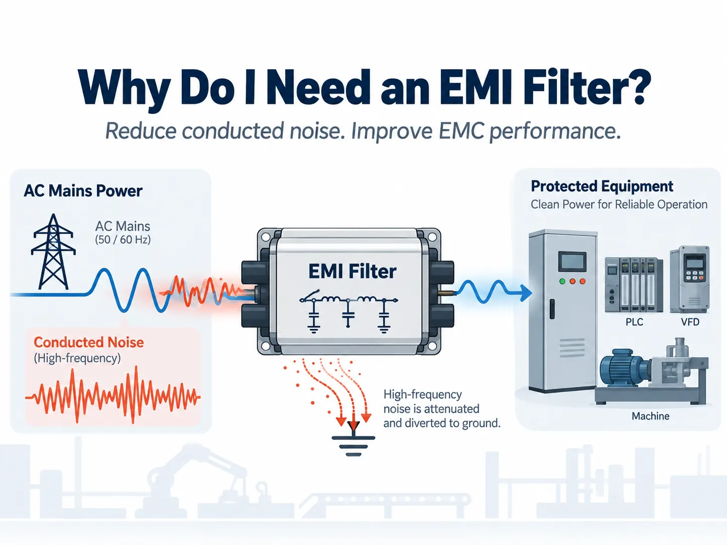
Primary noise sources include switching power supplies operating at frequencies above 150kHz, high speed digital signals with fast edge rates, and motor drives with commutator switching. This connects to electromagnetic compatibility because power line noise can propagate to other equipment sharing the same electrical circuit.
Primary noise sources include switching power supplies operating at frequencies above 150kHz, high speed digital signals with fast edge rates, and motor drives with commutator switching. This connects to electromagnetic compatibility because power line noise can propagate to other equipment sharing the same electrical circuit.
Radiated Emissions Failures
Radiated emission testing captures electromagnetic field strength from 30MHz to 6GHz using calibrated antennas in controlled test environments designed to absorb RF energy reflections.
Main emission sources include cables acting as unintended antennas, PCB traces carrying high frequency signals, and clock harmonic radiation from digital circuits. Building on conducted emissions concepts, power line noise often couples to attached cables, converting conducted interference into radiated emissions that exceed regulatory limits.
Transition: Understanding these fundamental test categories enables identification of specific design areas where failures most commonly occur.
Main emission sources include cables acting as unintended antennas, PCB traces carrying high frequency signals, and clock harmonic radiation from digital circuits. Building on conducted emissions concepts, power line noise often couples to attached cables, converting conducted interference into radiated emissions that exceed regulatory limits.
Transition: Understanding these fundamental test categories enables identification of specific design areas where failures most commonly occur.
Critical Design Areas That Cause EMC Failures

Design oversights in three critical areas account for approximately 80% of all emc test failures: power supply integration, PCB layout practices, and component selection decisions.
Power Supply and Cable Issues
Non-compliant power adapters represent a frequent failure source even when individual adapters carry compliance markings, because the combination of adapter plus product may exceed emissions class limits during final system testing.
Cable routing creates unintended antenna structures when multiple cables bundle together or when flex cable connections lack adequate main board ground connections. Poor cable management negatively affects both emissions and immunity performance by creating discharge paths for ESD events and coupling mechanisms for RF noise injection.
Inadequate filtering at the main power input allows switching noise to propagate through power supplies to other devices sharing the same electrical distribution, requiring common mode filters and differential filtering components.
Cable routing creates unintended antenna structures when multiple cables bundle together or when flex cable connections lack adequate main board ground connections. Poor cable management negatively affects both emissions and immunity performance by creating discharge paths for ESD events and coupling mechanisms for RF noise injection.
Inadequate filtering at the main power input allows switching noise to propagate through power supplies to other devices sharing the same electrical distribution, requiring common mode filters and differential filtering components.
PCB Layout Problems
Circuit board ground plane splits force high frequency return currents through longer, higher-impedance paths that increase both radiated emissions and susceptibility to external interference.
High speed digital signals routed between connector locations create direct coupling between internal PCBs and external cabling attached to the product, essentially using cables as transmitting antennas for clock harmonics and switching noise.
Large current loop areas formed by poor PCB layout practices increase magnetic field coupling and create emission sources that become problematic during radiated emission testing above 30MHz.
High speed digital signals routed between connector locations create direct coupling between internal PCBs and external cabling attached to the product, essentially using cables as transmitting antennas for clock harmonics and switching noise.
Large current loop areas formed by poor PCB layout practices increase magnetic field coupling and create emission sources that become problematic during radiated emission testing above 30MHz.
Component Selection Errors
LCD display modules from different manufacturers exhibit vastly different emission characteristics, with some displays generating significant RF noise that requires additional noise suppression beads or filtering to achieve compliance.
Ferrite components selected without consideration of specific frequency range requirements often provide inadequate suppression, particularly for conducted emissions below 1MHz where high-permeability materials perform better than standard ferrite beads.
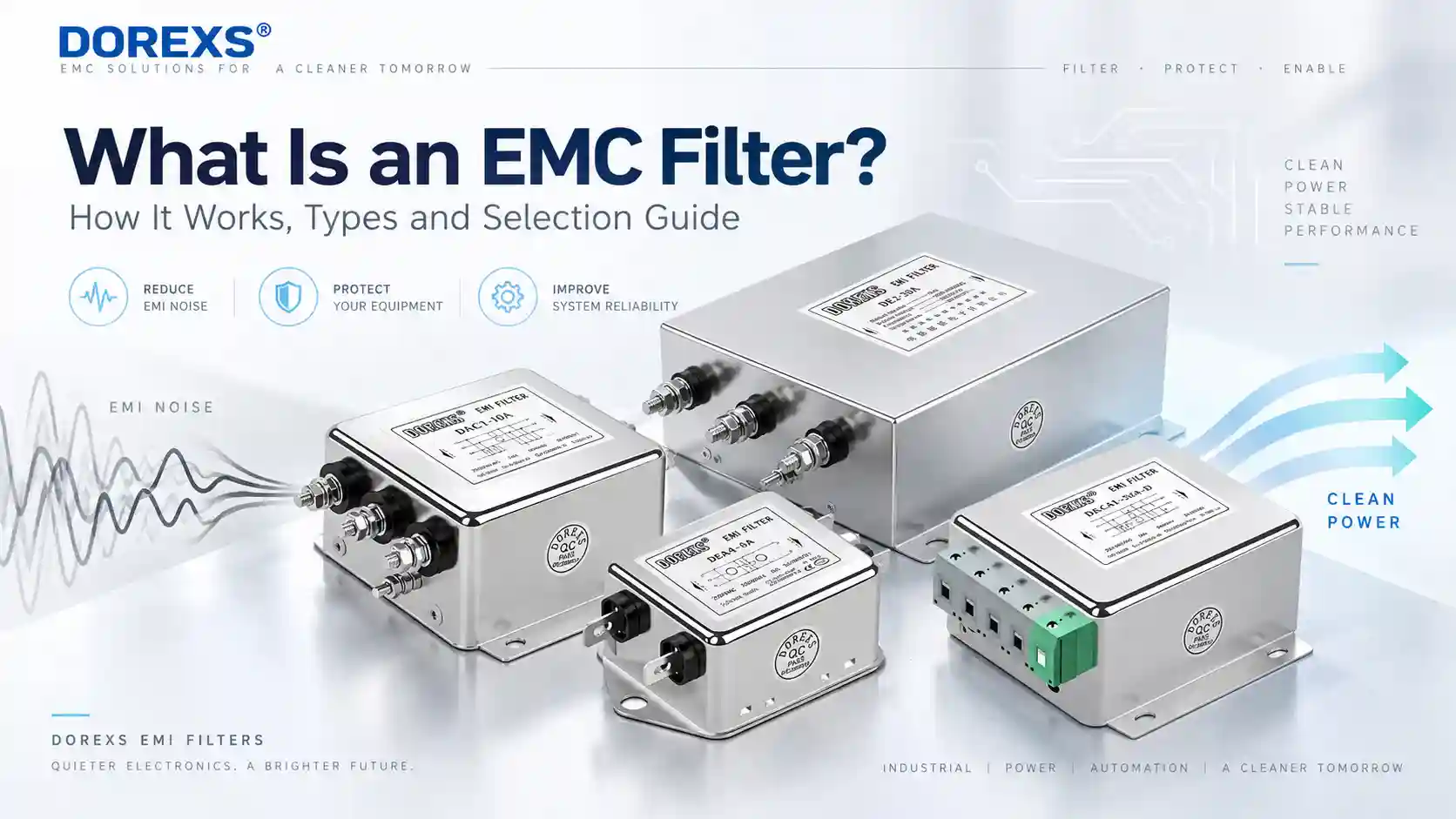
Missing EMI filter integration during initial design phases forces expensive retrofitting approaches, whereas early integration of quality filtering solutions like DOREXS EMI filters provides superior performance and cost-effectiveness compared to adding multiple discrete components.
Transition: Identifying these design weaknesses enables systematic prevention through proven troubleshooting and testing procedures.
Ferrite components selected without consideration of specific frequency range requirements often provide inadequate suppression, particularly for conducted emissions below 1MHz where high-permeability materials perform better than standard ferrite beads.
Missing EMI filter integration during initial design phases forces expensive retrofitting approaches, whereas early integration of quality filtering solutions like DOREXS EMI filters provides superior performance and cost-effectiveness compared to adding multiple discrete components.
Transition: Identifying these design weaknesses enables systematic prevention through proven troubleshooting and testing procedures.
Step-by-Step Troubleshooting and Prevention Methods
Systematic pre compliance testing during prototype development identifies potential EMC issues before formal certification testing, reducing the risk of expensive test house failures.
Pre-Compliance Testing Procedure
When to use this: During prototype development phase before submitting to accredited test lab for formal compliance testing.
-
Conduct near-field scanning: Use spectrum analyzers with near field probes to identify emission hot spots on circuit boards, connectors, and cable routing areas during normal product operation.
-
Isolate noise sources with current probes: Measure common-mode and differential-mode currents on all cables to identify which connections carry excessive RF noise requiring filtering or rerouting.
-
Test power adapter compatibility: Connect auxiliary equipment and test with multiple power adapter models to verify emissions class compliance across different supply configurations and dynamic load conditions.
-
Perform basic immunity testing: Use handheld ESD guns and RF signal generators for exploratory testing at key esd testing locations including connector shells, chassis ground points, and user interface areas.
Comparison: Quick Fixes vs. Design Changes
Approach |
Quick Fixes |
Design Changes |
|
Timeline
|
1-2 weeks implementation
|
6-12 weeks for PCB redesign
|
|
Cost Impact
|
$500-2000 for materials
|
$10,000-50,000 for tooling changes
|
|
Effectiveness
|
60-80% problem resolution
|
95%+ problem resolution
|
|
Examples
|
Ferrite beads, copper tape, cable rerouting
|
Circuit board layout changes, EMI filter integration
|
Quick fixes work effectively for minor emissions issues and immunity problems but may not address fundamental design flaws that cause multiple failure modes. DOREXS EMI filters should ideally be integrated during initial design phases for optimal performance, though they can also provide effective retrofit solutions for power supply filtering requirements.
Transition: These systematic approaches address the most frequent failure categories encountered during formal compliance testing.
Common EMC Challenges and Solutions
These four challenge categories represent approximately 80% of all emc test failures reported by accredited testing facilities, with solutions that prevent recurrence in future product designs.

Challenge 1: Conducted Emissions Above 1MHz Due to Switching Noise
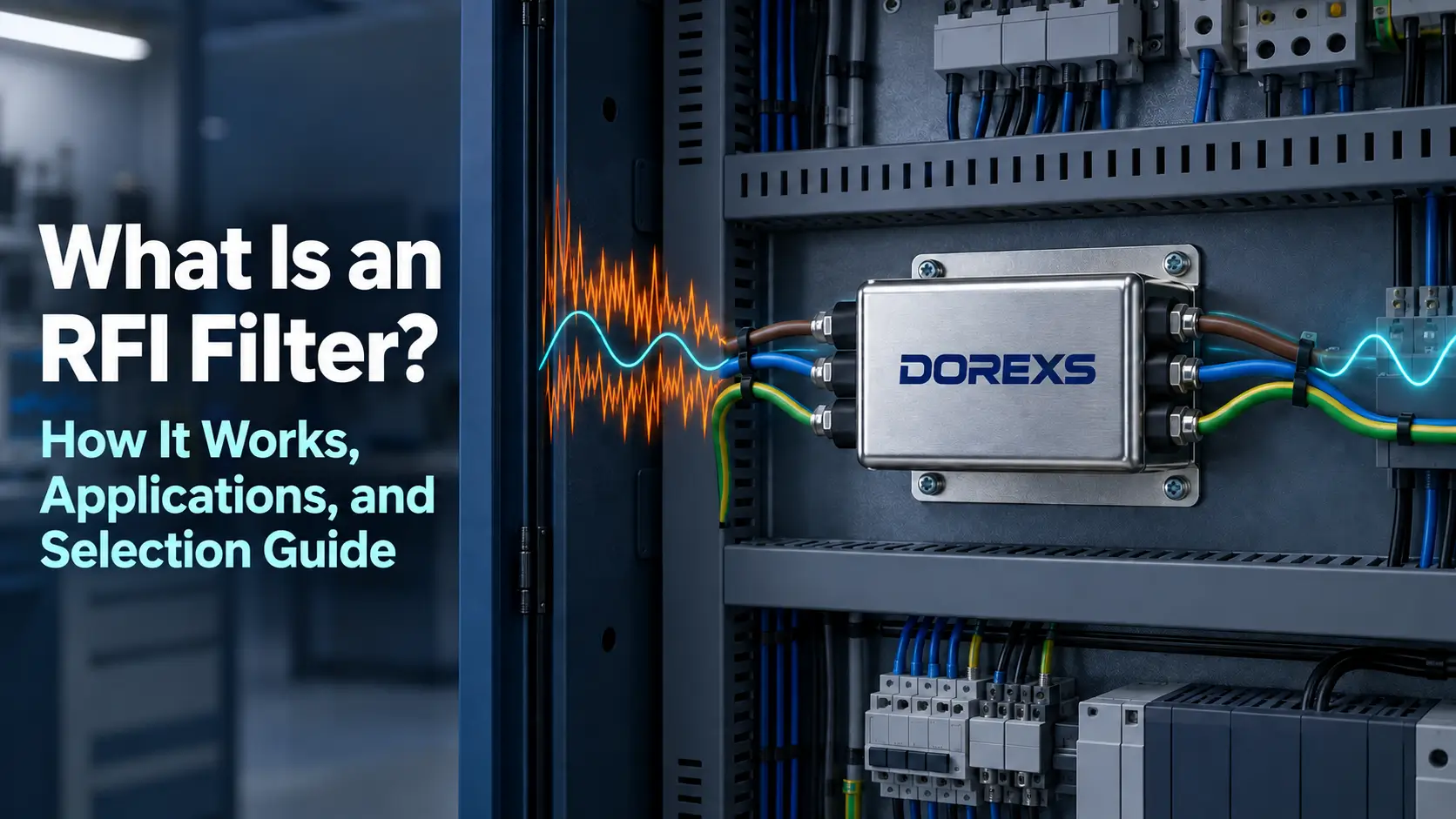
Solution: Install common mode filters and differential-mode filters at the main power input, with DOREXS three-phase or single-phase EMI filters providing robust filtering for industrial applications requiring high current capacity.
Additional measures include improving circuit board ground plane integrity and adding bypass capacitors near high-speed switching circuits to reduce rf noise at the source before it reaches power distribution networks.
Additional measures include improving circuit board ground plane integrity and adding bypass capacitors near high-speed switching circuits to reduce rf noise at the source before it reaches power distribution networks.
Challenge 2: Radiated Emissions from USB/Ethernet Cables Below 300MHz
Solution: Add ferrite noise suppression beads on cables near connector locations, improve connector grounding to chassis ground references, and minimize high speed digital signals trace lengths between DIP connector locations.
Cable management requires using shielded cables with proper 360-degree termination to well grounded conductive shield connections, preventing cables from acting as efficient radiating antennas.
Cable management requires using shielded cables with proper 360-degree termination to well grounded conductive shield connections, preventing cables from acting as efficient radiating antennas.
Challenge 3: ESD Testing Immunity Failures at 4kV and 8kV Test Levels
Solution: Install TVS diodes near connector grounds to provide controlled discharge paths, improve chassis bonding with multiple ground connections, and eliminate floating metal components that accumulate charge.
Design considerations include avoiding spark gaps between metal components and ensuring proper ESD protection circuitry routes discharge currents away from sensitive circuits on internal PCBs.
Design considerations include avoiding spark gaps between metal components and ensuring proper ESD protection circuitry routes discharge currents away from sensitive circuits on internal PCBs.
Challenge 4: Power Adapter Compatibility Issues
Solution: Test with multiple adapter models during development, verify that both adapter and product meet the same emissions class requirements, and add input filtering when the right power adapter selection alone cannot achieve compliance.
Specification requirements should ensure power adapters meet identical EMC requirements as the end product, preventing system-level compliance issues when testing products with auxiliary equipment connections.
Transition: These proven solutions provide the foundation for systematic EMC compliance approaches that prevent costly redesign cycles.
Specification requirements should ensure power adapters meet identical EMC requirements as the end product, preventing system-level compliance issues when testing products with auxiliary equipment connections.
Transition: These proven solutions provide the foundation for systematic EMC compliance approaches that prevent costly redesign cycles.
Conclusion and Next Steps
Systematic application of EMC design principles during initial development prevents 70% of compliance failures through proper power supply filtering, PCB layout optimization, and pre compliance testing validation before formal certification submission.
Early integration of quality EMI filter solutions and systematic troubleshooting approaches eliminates the expensive cycle of failed test reports, emergency design changes, and delayed product launches that characterize reactive EMC approaches.
To Get Started:
Early integration of quality EMI filter solutions and systematic troubleshooting approaches eliminates the expensive cycle of failed test reports, emergency design changes, and delayed product launches that characterize reactive EMC approaches.
To Get Started:
-
Perform pre compliance scanning: Use basic spectrum analyzers to identify emission sources on current prototypes before formal test lab submission
-
Review PCB layouts: Examine circuit board ground plane integrity, high-speed signal routing between connectors, and cable attachment grounding methods
-
Evaluate power filtering requirements: Consider DOREXS EMI filter integration early in design phases for robust conducted emissions compliance and improved immunity performance
Related Topics: EMI filter selection criteria for specific applications, advanced shielding techniques for sensitive circuits, and regulatory requirement updates for global market compliance including medical devices and short range device categories.
Additional Resources
Essential Test Equipment for Pre-Compliance:
-
Handheld spectrum analyzers with near-field probe sets for emission scanning
-
Current probe accessories for cable noise measurement
-
Basic ESD testing equipment for immunity validation
-
Power line impedance stabilization networks (LISN) for conducted emissions measurement
EMC Design References:
-
PCB layout guidelines for high-speed digital circuits and mixed-signal designs
-
Cable routing and connector grounding best practices for various product categories
-
Power supply filtering component selection guides including DOREXS EMI filter specifications for industrial and commercial applications
Medical Device EMC Requirements Explained Complete Guide to IEC 60601-1-2 Compliance
What Does EMI Stand For in Electrical? Explore Electromagnetic Interference